EXCLUSIVE FORUM FOR MACHINE DISMANTLERS AND REPAIR PEOPLE > Hammond
> Heavy Machinery
> Components
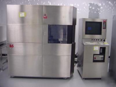
> Ivs - 200 wafer inspection system
Ivs - 200 wafer inspection system
Wafer Inspection System. An automatic metrology system designed to provide unattended sub-micron measurement of semiconductor features range of 0.1 to 200 microns
Feature Range: 0.1 to 20 microns
Feature Type : lines, spaces, multiple lines & spaces
Precision: Less or equal 7 nanometers, 3 sigma dynamic repeatability or 0.1% whichever is greater
Feature types: Contact holes and vias
Precision: Less or equal 20 nanometers 3 sigma dynamic repeatability or 1%, whichever is greater
Magnification: 100x to 200,000x
Acceleration Voltage: 0.5 KeV to 1.2 KeV
Resolution: 10nm at 1.0 KeV Scan Rates: 22.5 fps, not-interlaced
Cleanliness: Class 1 compatible
Wafer Size: 100mm, 125 mm and 200 mm SEMI standard wafers for Photomasks and Thin Film Heads 3 Cassette stations: 2 for production, 1 for standards. Pick and place robot and pre-aligner Auto template illumination. Automatically set template illumination during recipe setup Separate Measurement Module and Control Console